Create Your First Project
Start adding your projects to your portfolio. Click on "Manage Projects" to get started


Design, Simulate and Analyze the RF Microwave amplifier using S-parameter for FET device ATF 36077 f
Date
2023
Microwave amplifiers are renowned for their robustness, cost-effectiveness, and compact form factor, in addition to their broad frequency bandwidth and moderate power handling capacity. Semiconductor devices such as Si-based BJTs, GaAs-based HBTs, FETs, and HEMTs are used in the construction of low-noise amplifiers. Humanity is constantly pushing the boundaries of innovation in the realm of telecommunications. The proliferation of 5G technologies has served to accelerate the development of microwave and RF equipment, such as amplifiers, filters, mixers, and other analogous components. Amplifier is an important component for communication systems which is used at the end of the transmitter and the beginning of the receiver. The design techniques for BJT and FET amplifiers make extensive use of the concepts developed during the study of microwave transmission lines, two-port networks, and Smith chart representation. The discussion of transistor amplifier design on this paper will be based on the S-parameter representation of terminal characteristics. The amplification of received signals in microwave systems is an essential function that is fulfilled by microwave amplifiers.
II. DESIGN SPECIFICATION AND CONSIDERATION
This section contains the design of an amplifier that operates at a frequency of 3GHz. The amplifier's design will be based on the S parameter values specified in the datasheet provided. The discussion in this section will encompass the stability of the amplifier, stability circles, the maximum permissible source and load reflections, maximum gain attainable, as well as the input and output matching networks of the amplifier.
A. Specifications of Design
• Operating frequency = 3 GHz
• Microstrip line with substrate of 4.5
• Thickness 1.6 mm
• Loss tangent = 0.019
For the transistor FET ATF 36077,
The biasing voltage and current are VDS = 1.5V and IDS = 10 mA
S-parameter
Values
S11=0.94∠-49°
S21=4.745∠ 132°
S12=0.043∠54°
S22 =0.57∠-41°
B. Stability of the Amplifier
We know that, if the value of K is greater than 1 and the value of 𝛥 is less than 1, the amplifier is considered to be unconditionally stable, meaning that any value on the Smith chart results in a stable gain. In the current case, the amplifier is conditionally stable, as K is lesser than 1 and 𝛥 is less than 1.
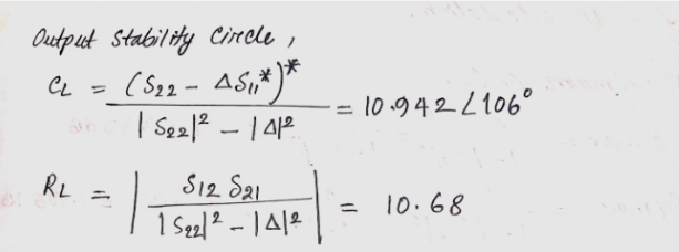
C. Stability Circle
Stability circles are used to show the regions of 𝛤S and 𝛤L that are stable and those that are potentially unstable. Subsequently, the calculated values are plotted on the Smith chart.
III. SIMULATION OF AMPLIFIER
Once the calculations are finished, it's important to verify their validity by comparing them with the simulation results from the AWR Design environment. The figure represents a circuit designed using the schematic function of the AWR software and the FET device ATF-36077. This design will be utilized to evaluate the S-parameters.
IV. DISCUSSION
The design involves the use of the ATF-36077 FET device, which was created with the AWR software. Before proceeding with the design, it's necessary to thoroughly review the datasheet for this device.
The S-parameters are used to calculate K and Δ to evaluate the stability of the system, and it is found to be conditionally stable as both K and Δ are less than 1. The input and output stability circles are then plotted in a smith chart using the values of RS, CS, RL, and CL.
Bilateral s-parameter method was not a practical solution, as it led to values of 1 for gamma_s and gamma_l, which made it challenging to calculate the location and length at the source and load on the smith chart.
The device operates in the unilateral mode, as indicated by the maximum gain constant and S12 being equal to 0. The assumption of ΓS = ΓOPT = 0.832∠52.71 for the smallest possible noise figure is made. For the output section, the value of ΓL = S22* = 0.57∠41 is chosen.
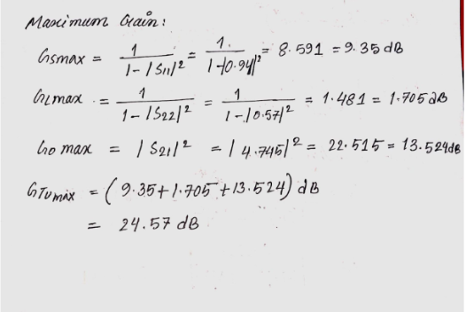
The matching circuit is then determined using the smith chart, and the design is further developed using AWR software. The results of the manual calculations and the software simulations are compared, and the differences are found to be 2.37 dB, which might be due to circuit loss and the estimated value of Gamma opt. Despite attempting to incorporate a low noise amplifier into the design, it proved to be difficult to plot the constant gain and noise figure circles. Hence, the results obtained by assuming ΓS = ΓOPT and ΓL = S22* are considered reliable.
To put it briefly, the maximum gain amplifier design is shown in a step-by-step process, both manually and using software. The results from these two methods are then compared and found to be close, with a small difference of 2.37 dB. Overall, the design is considered dependable, but further research is necessary to incorporate noise parameters.